6 Critical Steps Involved in the Manufacturing Metal Core PCBs
6 Critical Steps Involved in the Manufacturing Metal Core PCBs
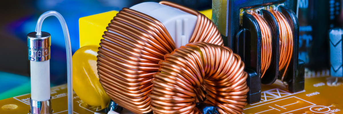
Metal Core PCBs play a crucial role in numerous electronic devices and systems, particularly in industries like automotive, aerospace, and power electronics. These applications demand exceptional thermal conductivity and dependable heat dissipation, which metal core PCBs provide. Different from conventional PCBs, metal core PCBs feature a base made of aluminum or copper that functions as a heat sink, enabling effective temperature regulation for electronic components. Are you interested in learning about the manufacturing process behind these types of PCBs?
Steps Involved in the Making of Metal Core PCBs
The making of metal core printed circuit boards encompasses a series of crucial steps aimed at producing top-notch circuit boards that excel in heat dissipation for applications demanding optimal efficiency. The following are the fundamental stages involved in the production process of these types of PCBs.
These steps involve a combination of precision machinery, chemical processes, and quality control measures to making metal core printed circuit boards that meet the required specifications for efficient heat dissipation and unmatched electrical performance. Therefore, in order to get the finest quality metal core PCBs, it is recommended to partner with reputable and industry-leading manufacturers like Twisted Traces that have the expertise, knowledge, and resources to deliver high-quality metal core PCBs that meet strict industry standards.
-
Design and Layout: The initial phase of Metal Core PCB fabrication involves designing and laying out the circuit board. This process encompasses creating a comprehensive schematic diagram of the intended circuit and determining the optimal placement and routing of its components.
-
Material Selection: After the design has been approved, the next stage is carefully selecting the suitable materials for the PCB. This process usually involves making decisions on metal core materials like aluminum or copper, as well as substrate materials and any supplementary layers necessary for the particular application.
-
Etching and Lamination: The etching and lamination stage is the third step in the manufacturing process. During this phase, a layer of copper is applied to the metal core material and then excess copper is removed through etching to form the desired circuit pattern. Lamination is subsequently utilized to securely bond all layers of the PCB together.
-
Drilling and Plating: Following the etching and lamination procedure, the printed circuit board (PCB) undergoes a process of hole drilling to facilitate component positioning. Also, these holes are coated with copper to guarantee effective electrical connectivity and establish solder pads for secure component attachment.
-
Solder Mask and Silkscreen: The next step is the application of a solder mask, which is a protective layer that covers the copper traces on the PCB. This helps to prevent solder bridges and guarantees proper soldering during assembly. A silkscreen layer is also added during this step to provide component labels and other necessary markings.
-
Testing and Inspection: Once the PCB is fully assembled, it undergoes rigorous testing and inspection to ensure that it meets the required specifications and quality standards. This typically involves electrical testing, reliability testing, and visual inspection.
.png)

