
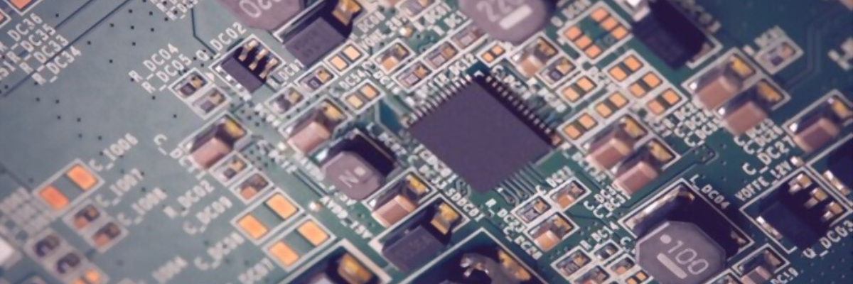
With the increasing demand for high-speed, performance-driven, yet miniature devices, manufacturing and assembling printed circuit boards (PCBs) have gained immense traction. This is because PCBs drive the functioning of all electrical and electromechanical devices. Hence, PCB design should be flawless and precise for the further execution of processes, including component mounting, vias, circuits, and more. Vias play a crucial role in PCB design, especially in multilayer boards. Vias guarantee ease of routing and enable the circuit boards to be made as per the design. However, they are more than just interfaces for physical and electrical routing. PCB vias should be designed with exact dimensions to comply with industry manufacturability and assembly standards. Today, blind and buried vias are widely incorporated into PCB designs to improve functionality and signal performance and reduce overall board size. Are you intrigued to know more about these vias and the design considerations for incorporating blind and buried vias in PCBs? If yes, this post is for you. Stay, tuned.
Vertical interconnect access or vias are plated through-holes in a circuit board. They provide the physical and electrical connections between components on a PCB. Depending on the application requirements, vias can be drilled mechanically or by laser. PCB vias are a crucial part of multilayer PCBs that are complex to design. Today, different vias are used – blind and buried are popular among them.
Both, blind and buried vias have their specific design rules. The following section describes the same in detail.
By now, you may have got some clarity regarding incorporating blind and buried vias in PCBs. The aforementioned vias design rules increase the circuit board density and cut the production cost. These design-related advancements enables PCB manufacturing processes to be flawless, especially in case of high-density designs. However, the requirement should be done appropriately to get the desired outcome. Would you like to work on electronics projects that involve complex PCB designs? If the answer is yes, then these guidelines might help. Additionally, you may consult an industry expert for any further questions or assistance. Twisted Traces is a one-stop solution that can offer you PCB assemblies with complex designs, several components, and multiple layers. The company utilizes suitable vias processes for designing and manufacturing PCBs. The company is known for offering end-to-end manufacturing and assembly solutions.
.png)
