RF PCBs – Materials Used and Design Stack-up Explained
RF PCBs – Materials Used and Design Stack-up Explained
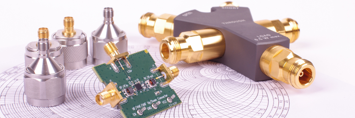
Radio frequency (RF) printed circuit boards (PCBs) have been an integral part of electronics industry for several year now. These PCBs are designed to operate in their specified megahertz to gigahertz frequency ranges. Therefore, they are widely used in mission-critical applications such as military radar, cellular phone operations, networking and communications, and more. However, facilitating the transmission of high-frequency signals and achieving optimal performance in RF circuits demands attention to the material selection and configuration of the PCB stack-up. Would you like to know how the RF circuit is stacked up? What materials are used for RF PCBs? This post answers these questions in detail.
Types of Materials Used for RF PCBs
Different types of materials are used in the construction of RF PCBs. Each is differentiated based on its strengths and characteristics. Some of the most prevalent materials are described below.
-
FR-4 (Fire Retardant-4): This is one of the most commonly used materials in the PCB industry, mainly because of its versatility and cost effectiveness. The material comprises woven fiberglass cloth filled with an epoxy resin binder. Although FR-4 is an ideal choice for many low-frequency applications, its dielectric properties may degrade at higher frequencies due to its high dielectric constant (Dk) and dielectric loss (Df).
-
PTFE (Polytetrafluoroethylene): PTFE-based materials offer excellent electrical properties, including stable and consistent performance and low dielectric loss over various frequencies. Therefore, they are ideal for high-frequency RF applications with paramount signal integrity. However, these substrates tend to be more expensive than FR-4.
-
Rogers Laminates: Rogers Corporation is renowned for producing high-performance laminates, specially engineered for RF and microwave applications. These laminates consist of hydrocarbon-based or ceramic-filled substrates with precise control over dissipation factor, dielectric constant, and thermal stability. Compared to FR-4 materials, these laminates offer superior electrical properties required in RF circuitry.
-
Ceramic Substrates: Most high-power RF applications demand ceramic substrates such as alumina (Al2O3) or aluminum nitride (AlN). These substrates provide excellent thermal conductivity, allowing efficient heat dissipation, and can withstand high power levels without degradation. They are commonly used in RF filters, RF power amplifiers, and antenna systems.
Detailed Discussion on Designing RF PCB Stackup
An RF PCB stack-up design requires a clear understanding of application requirements and considerations of various factors such as signal integrity, impedance matching, electromagnetic interference (EMI) mitigation, and so on. Here are some essential pointers that will help you in designing an effective RF PCB stack-up:
-
Defining the design requirement is the first and foremost important step in the RF PCB stackup. Clearly understand and define your RF system's requirements, including signal bandwidth, frequency range, power levels, and environmental conditions.
-
Another important step is determining the number of layers and materials being used. RF circuits benefit from a multilayer stack-up as it provides sufficient ground and power planes for signal integrity and RF isolation. Make sure the material being used has the appropriate loss tangent (Df), dielectric constant (Dk), and thickness for your RF frequency range. FR-4, Rogers, and Teflon-based materials are some commonly used materials for RF systems.
-
Once you have completed the layer count, plan the arrangement of signal, ground, and power layers. In standard RF stack-ups, ground planes surround signal layers to minimize interference and provide controlled impedance.
-
Next, implement a ground plane on each layer. This will help minimize ground loops, reduce EMI, and provide a reference for controlled impedance traces.
-
Considering the application requirements and substrate properties, determine the required characteristic impedance for RF transmission lines. Utilize controlled impedance routing techniques and ensure layer stack-up and consistent trace widths for impedance matching.
-
Ensure RF signal traces are placed on inner layers between ground planes to provide isolation and shielding. Refrain from routing high-speed signals across split planes to minimize crosstalk and EMI.
-
Design multiple power distribution planes to provide clean and stable power to RF components. This will separate analog and digital power domains and minimize noise coupling.
-
Carefully strategize the spacing between components to minimize signal path lengths, reduce parasitic effects, and optimize signal integrity. Consider component orientation for optimal RF performance and thermal management.
-
Implement shielding, filtering, and proper grounding to minimize electromagnetic interference from radiated and conducted sources.
-
Use thermal management techniques such as thermal vias, heat sinks, and proper component placement to dissipate heat generated by RF components and maintain reliability.
-
Document every detail regarding the stack-up design, including material properties, layer stack arrangement, controlled impedance values, and any special considerations for manufacturing and assembly.
-
Fabricate a prototype based on the finalized stackup design and perform testing to validate RF performance under real-world conditions.
With the ever-evolving RF technology and wireless communications, the design of RF PCBs is an enabler of reliability and performance. Experts can unlock the potential of these circuits in the future by adequately selecting materials and configuring the stack-up to meet the specific requirements of high-frequency operations. If you want to create an RF PCB stack-up for your application, collaborating with experienced PCB manufacturers and assemblers will ease your task. Twisted Traces is a prominent player in this segment and stands out among its competitors. Our team of experts will assist you throughout the process, from material selection and design to assembly. Also, they offer custom options. Contact us today to share your RF PCB stackup requirements. The experts will get back to you with a possible solution.

.png)
