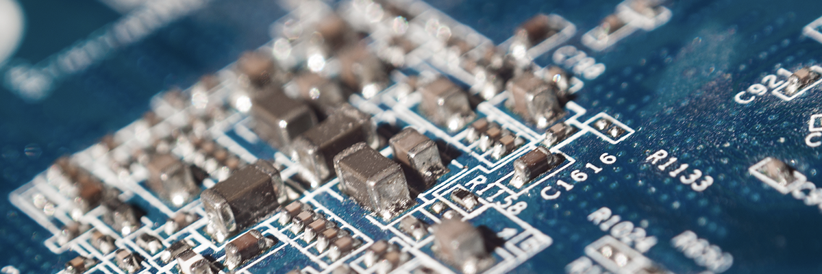

Silkscreen printing is an indispensable part of the printed circuit board fabrication. If you are new to the field of PCB design and fabrication, you must be wondering about the significance of this printing process. The silkscreen is a layer of ink traces that helps provide text-based, human-readable information of different circuit points, components, and additional circuitry, date codes, testing points, and manufacturer marks, among others. Silkscreen, also known as legend or nomenclature, allows both the manufacturer and the engineer to locate and identify all the components, while also eliminating the chances of errors. How is silkscreen applied to PCBs? There are majorly three methods. Let’s see the methods in brief in this post.
Being one of the most artistic processes in a PCB manufacturing, the silk-screening process requires specially formulated inks. Almost every silkscreen circuit board manufacturer applies silkscreen through any of the following methods:
Silkscreening is used during different phases of PCB manufacturing and assembly. It is mainly used during mounting or placing components. The following are a few silkscreen indicators used to position the components.
The silkscreen markings are also used during the inspection and testing phase of the PCB manufacturing. They are used to mark the following:
Following these markings enable PCB fabricators to detect component failures, as well as verify the performance of the circuit board.
The whole process of screen printing is not too difficult, but it must be executed carefully to avoid errors. The quality and readability of silkscreen printing is more important than ever with the increasing complexity of today’s boards. Hence it is extremely crucial to get the printing done from an experienced silkscreen circuit board manufacturer like Twisted Traces. The team at Twisted Traces is experienced in all three forms of silk screening application methods as mentioned above. The experts at Twisted Traces suggest the most appropriate silk screening method after analyzing the specifications and other requirements.
