
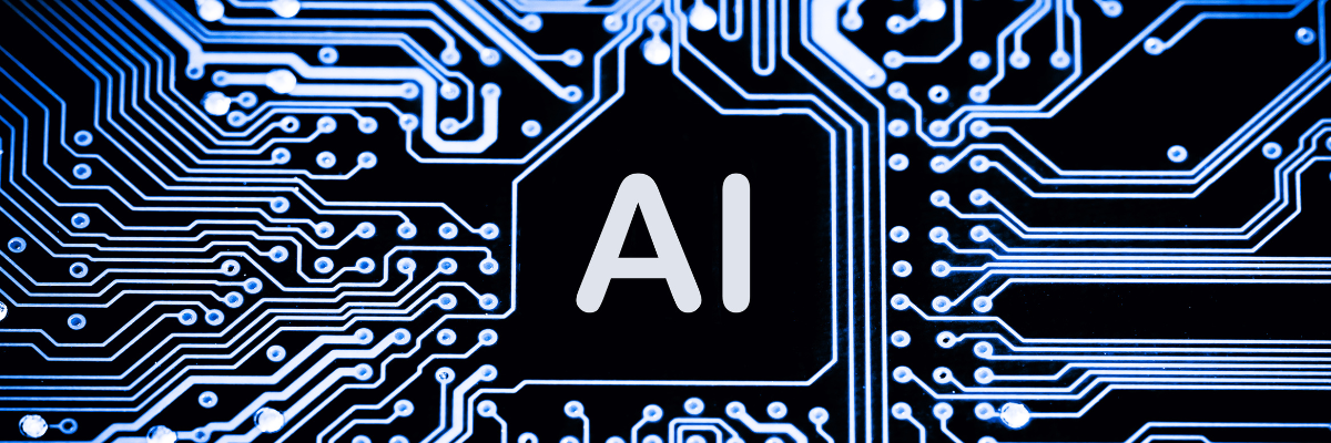
The rise of AI in PCB design marks can be attributed to the increasing demand for high-volume production of circuit boards for use across industries. Another driving factor for AI implementation in PCB design is the rising complexity, intricate wiring, and increase in the number of components. AI technologies have transformed the way PCBs are designed, shifting from manual, error-prone processes to highly automated and accurate operations. By adopting AI, companies are achieving unprecedented efficacy and precision in circuit design, component placement, and testing. This evolution not only speeds up the PCB development cycle, but also improves the dependability and performance of electronic devices. Moreover, AI’s ability to learn and adapt continues to refine the design process, reducing expenses and environmental impact by decreasing waste. This blog discusses about how AI has revolutionized the PCB design process, thus enhancing efficiency, accuracy, and innovation in the electronics industry, ushering in a new era of excellence.
AI has substantially transformed different aspects of the way PCBs are designed, changing layout automation, rule checking, and optimization methods. In layout automation, AI algorithms help in placing and routing components efficiently on the PCB. This not only accelerates the design methods but also ensures optimal use of space, and decreases the size and cost of the PCB. AI-powered tools use machine learning models to learn from huge datasets of existing designs, enabling them to suggest layouts that maximize performance while adhering to manufacturing requirements. Moreover, AI contributes by automating the verification of electrical and physical parameters against predefined design rules. This minimizes the requirement for manual inspections, drastically cutting down on the time and labor involved in detecting and correcting errors. Furthermore, AI optimizes continually by learning and adapting to new data, permitting it to provide suggestions for reducing power consumption, and enhancing signal integrity and thermal management. These factors signify the integration of AI in PCB as it helps drive efficiency, decrease errors, and foster innovation.
Implementing AI in PCB designs offers several benefits. Here are some relevant pointers.
Emerging Trends and Technological Breakthroughs Achieved by AI in PCB Designs
Here are some emerging trends in this segment.
Are you looking for top-notch PCB design and assembling service providers? Twisted Traces has you covered! We offer excellent layout, PCB fabrication and assembly that can be tailored to suit your requirements. Boost your projects with their expertise. Contact their sales team today to get started on your next electronic masterpiece.
.png)
