Understanding Sequential Lamination in HDI PCB Manufacturing

Understanding Sequential Lamination in HDI PCB Manufacturing
High-density interconnect (HDI) printed circuit boards have gained immense traction over the years. This is owing to their ability to accommodate more components and connections in a compact size. These PCBs have thinner boards and denser wiring per area than most conventional boards. The number of layers is also relatively less. This reduces the size and weight of the board without compromising on technological advancements and functionalities. They have high circuit density because of laser-drilled stacked micro-vias, blind/buried vias, and via-in-pads techniques. These features can be achieved by using sequential lamination. This is a crucial part of the HDI PCB fabrication process, wherein dielectric is inserted between an already laminated sub-composite and copper layers. This technique can create complex multilayer structures with precise interconnections, which are compact and lightweight, and used in advanced electronic devices. Are you intrigued to know how sequential lamination is used in HDI PCB manufacturing? This post discusses the process and its advantages in detail. So, stay tuned.
Overview of Sequential Lamination
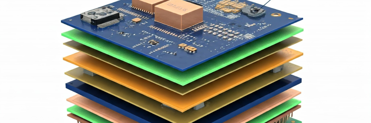
It is a specialized and intricate manufacturing process widely preferred to build HDI PCBs. It involves the layering and bonding of multiple cores and prepregs together, forming a complex structure. Although it is a multi-layer structure, each layer has a different design, consisting of traces, vias, and pads, and is laminated in sequence. Sequential lamination enhances signal integrity and plays a crucial role in advancing technology by enabling powerful and highly integrated electronic devices. The next section describes a step-by-step breakdown of this technique.
How Sequential Lamination is Performed for HDI PCBs?
The following pointers will help you understand this aspect.
-
Design and Material Selection: Sequential lamination begins with the design phase. Designers are responsible for determining the number of layers, their specific layout, and the placement of components. Here, the biggest challenge for designers is to fit everything in a limited space and minimum thickness. The next crucial step is material selection. The choice of substrate material, copper thickness, and prepregs can significantly impact the circuit board's performance. The sequential lamination process demands materials that can withstand high temperatures and pressures.
-
Preparing the Core Layers: The core layers are important structural components of HDI boards. The core layers are composed of high-quality laminates with a copper layer on each side to create the necessary circuitry, including traces and vias.
-
Adding Prepregs: They are used to insulate and bond the core layers. Prepregs are made using resin-impregnated glass fiber or other dielectric materials. Their primary function is to provide electrical insulation and mechanical support, and help maintain the spacing between layers.
-
Sequential Lamination: The core layers and prepregs are stacked and bonded individually in this step. This is accomplished using a hydraulic press, which applies heat and pressure to cure the prepregs and create a solid, multi-layered structure. This process is repeated until the multiple interconnected layers are formed. This makes the intricate circuitry required for HDI PCBs.
-
Drilling and Plating: Once the lamination is done, holes are drilled in the circuit boards to create vias. These vias connect different layers and are plated with copper to ensure correct electrical connections.
-
Etching and Finishing: The extra copper on the surface is etched away to unveil the intended circuitry. Next, the circuit board is finished with a silkscreen and solder mask to protect the traces and provide labeling.
-
Testing and Quality Control: The final board undergoes several rigorous testing and quality control procedures to ensure it meets the required specifications. Electrical testing to verify the circuitry's functionality and check for defects is one such testing procedure.
Sequential Lamination Advantages Discussed
Sequential lamination offers several advantages, which immensely contributed to their popularity.
-
Improved Signal Integrity: The signal integrity is enhanced with smaller traces and vias. This helps in reducing interference and noise in high-speed circuits.
-
Complex Designs: Sequential lamination can accommodate complex and highly customized PCB designs, making it a preferred option for various applications.
-
Miniaturization: This manufacturing technique enables the creation of smaller, more compact PCBs, which is a critical and much-in-demand factor in the design of portable devices.
-
Higher Layer Counts: This is another benefit offered by sequential lamination. This allows for more layers in a PCB, which is essential for achieving the desired density in modern electronics.
-
Reliability: High-quality materials and controlled manufacturing conditions ensure the reliability and durability of HDI PCBs.
-
Cost Effectiveness: Although it is a specialized process, it can be cost-effective in the long run as the size and complexity of a device's overall design reduce.
Sequential lamination is a key process for building multi-layer stack-ups in HDI PCBs. The significance of this technique is huge in modern electronics and will remain a driving force in shaping the industry's future. If you need HDI PCBs for your upcoming electronics application, it is important to consult a reliable, industry-leading PCB manufacturer and assembler who can cater to your requirements. Twisted Traces stands tall among its other competitors. The company caters to specific and custom requirements concerning HDI PCBs and uses sequential lamination as well. For any further questions, you can contact our team of experts.

