Why Component-to-Edge Clearance is Key to Effective PCB Design?
Why Component-to-Edge Clearance is Key to Effective PCB Design?
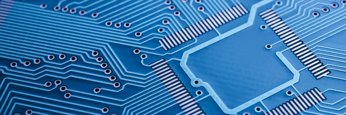
In electronics manufacturing, where every minute detail counts, the printed circuit boards (PCBs) design is a crucial step that requires an eye for detail to make devices work as expected. Errors such as placing a component too close to the edge, can cause significant problems. Component-to-edge clearance isn’t just a minor detail -it’s a critical factor that affects how well PCB performs, how long it lasts, and how easily it can be manufactured. Understanding component-to-edge clearance ensures PCBA functions effectively and fulfills the challenging demands of manufacturing and real-world use. This blog highlights the role of component-to-edge clearance in maximizing PCB efficiency.
Why Component-to-Edge Clearance Matters?
Several aspects of a product design and functionality as well as basic safety requirements influence of component-to-edge clearance. Here are some of them.
-
Manufacturing Tolerances: PCB manufacturing processeshave tolerances that need to be accounted for. These tolerances can occur due to factors such as drilling, cutting, or component placement. Ifcomponents are too close to the edge, any variations may affect these processes.This can cause issues during assembly or affect the functionality of the board, resulting in potential failures or defects in the final product.
-
Mechanical Stability: Adequate space between components and the edge of the PCB is crucial for maintaining the board’s mechanical stability. This clearance protects components from damage that can occur during the different stages of production and prevents them from getting knocked off or damaged in the field.
-
Electrical Safety: Placing components too close to the PCB edge can lead to electrical issues, such as short circuits.This can cause the device to malfunction or fail. Keeping components awayfrom the edge also helps improve the board’s electromagnetic compatibility(EMC). By maintaining proper clearance, the PCB can operate safely andreliably.
-
Compliance with Standards: Different standards should be considered while designing the PCB. IPC-2221 is one of them. By adhering to these standards, designers can ensure that their PCBs meet the necessary quality and safety benchmarks, reducing the risk of product failures and ensuring compatibility with new or existing components and systems.
Achieving Component-to-Edge Clearance: Essential PCB Design Strategies
Several vital rules should be considered when designing a PCB with components-to-edge clearance. This ensures the reliability, manufacturability, and mechanical integrity of the board. Here are some important design considerations:
-
Component Placement and Clearances:To prevent damage during handling and manufacturing, ensure that allcomponents are placed at least 0.1 inches (2.54 mm) away from the boardedge. For larger components, such as connectors or edge-mounted parts,increase this clearance to a minimum of 0.2 inches (5 mm) to avoid mechanical stress and potential damage.
-
Panels with V-grooves: Ensure components are placedat least 0.05 inches (1.27 mm) away from the V-groove to prevent damage or unpredictable board breaks during the snapping process. Additionally,maintain a minimum clearance of 0.02 inches (0.5 mm) for copper traces andpads to avoid damage during board separation.
-
Panels with Breakout Tabs:Maintain a minimum clearance of 0.1 inches (2.54 mm) between component sand breakout tabs to protect them from mechanical stress during braking.Additionally, ensure at least 0.05 inches (1.27 mm) of clearance for copper traces and drilled holes to prevent damage during depanelization.
-
Copper Traces near Board Edge:Maintain a minimum clearance of 0.02 inches (0.5 mm) between coppertraces, including ground planes, and the board edge to prevent shorts andensure copper integrity during depanelization. If edge plating isrequired, ensure traces do not extend directly to the edge, allowing adequate space for the plating process.
-
Mechanical Support and Stability: Place mounting holes at least 0.125 inches (3.175 mm) from the board edge,reinforcing the area with larger copper pads if mechanical stress is anticipated. For PCBs exposed to significant mechanical stress, consider adding edge rails or additional support structures to help distribute the load effectively.
-
Thermal Considerations: Place thermal pads or heatsinks away from the board edge for components that generate significant heat to prevent uneven cooling and mechanical stress. Additionally,position heat-sensitive components further from the edge to ensure proper cooling, as edge-mounted components may not dissipate heat as effectively.
-
Drilled Holes: To prevent the weakening of the PCB edge and avoid cracking during mechanical assembly, place drilled holes (for screws, mounting, and more) at least 0.1 inches (2.54 mm) from the board edge. For routed boards, maintain a minimum clearance of 0.05 inches (1.27 mm) from the board edge for all components, traces, and holes to ensure clean cutting and prevent damage during the routing process.
Component-to-edge clearance is not a minor aspect in PCB design; it is a vital factor that influences electronic devices' overall reliability, functionality, and manufacturability. By adhering to the essential design strategies, designers can significantly reduce the risk of mechanical failures, electrical issues, and manufacturing defects. If you are looking for a reliable partner who will take PCB design to the next level, Twisted Traces is the right place. The experts here ensure attention to detail, including component-to-edge clearance, for maximum PCB performance and reliability. From design to assembly, you can rely on us.

.png)
